Key Takeaways...
- PCBs are manufactured through a multi-step process including design, etching, drilling, plating, and testing.
- Substrate materials and copper layers form the structure, while solder masks and silkscreens finalise the board.
- Each step requires precision and quality control to ensure electronic functionality.
- The metals and materials used in PCBs contribute to their recyclability and value.
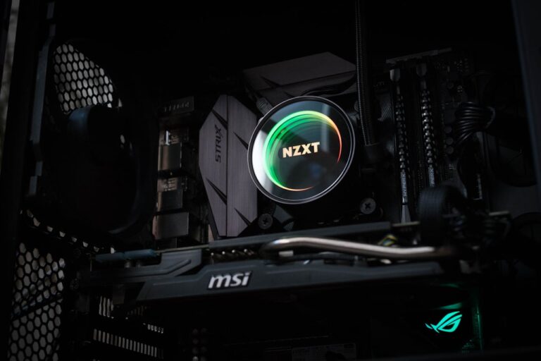
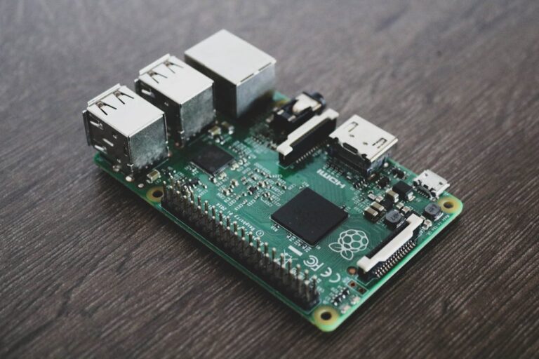
Printed circuit boards (PCBs) are the backbone of modern electronics. From smartphones and laptops to medical devices and industrial equipment, PCBs enable the complex functionality we rely on daily. But how exactly are these intricate boards created?
In this article, we walk through the full PCB manufacturing process—from raw materials to the finished board—explaining how each step contributes to the structure and function of a PCB. Whether you’re an engineer, recycler, or business professional, understanding this process is crucial for making informed decisions about design, sourcing, and responsible disposal.
Step 1: PCB Design
The manufacturing journey begins with the circuit design. Using CAD (computer-aided design) software, engineers lay out the circuitry, component placements, and electrical pathways. This design is then converted into Gerber files, the standard format for PCB production. These files guide every step of the fabrication process, ensuring the board functions as intended.
The design includes details such as:
- Number of layers (single-layer, double-layer, or multi-layer)
- Dimensions of the board
- Hole and drill locations
- Copper trace widths
- Component mounting locations
Step 2: Substrate Preparation
The base material, or substrate, is usually made from fibreglass-reinforced epoxy resin (FR4). This non-conductive layer provides structural support. A thin sheet of copper is laminated on one or both sides of the board to form the conductive layer. Multi-layer PCBs are formed by stacking and bonding multiple layers of substrate and copper.
This foundational step sets the stage for all further processing, determining the board’s flexibility, heat resistance, and mechanical durability.
Step 3: Image Transfer and Etching
Next, the copper is patterned according to the PCB design. A photosensitive film (photoresist) is applied to the board, and ultraviolet light exposes it using a stencil derived from the Gerber file. This hardens the areas where copper traces will remain.
The unexposed areas are then removed chemically, and the board is placed in an etching solution to dissolve the excess copper. What’s left are the precise copper pathways that will connect various components on the board.
Step 4: Drilling and Plating
Drilling is used to create holes for component leads and vias (electrical connections between layers). These holes are made with CNC machines to micrometre accuracy.
After drilling, the holes are electroplated with copper to establish conductivity between layers. This step is crucial for multi-layer boards and enables the flow of electricity throughout the circuit.
Step 5: Solder Mask and Silkscreen
A solder mask is applied to insulate the copper traces and prevent accidental short circuits. It also leaves component pads exposed for soldering. This layer typically comes in green, but other colours are possible.
Next, the silkscreen layer is printed. It contains symbols, text, and labels that assist in component placement and identification during assembly and repair.
Step 6: Surface Finish
To ensure proper soldering of components, a surface finish is applied to exposed pads. Common finishes include HASL (Hot Air Solder Leveling), ENIG (Electroless Nickel Immersion Gold), and lead-free options.
Each surface finish offers different benefits in terms of durability, conductivity, and compatibility with automated assembly processes.
Step 7: Electrical Testing and Quality Control
Before shipping, the PCB undergoes electrical testing to check for shorts, open circuits, and other defects. High-voltage probes trace the circuitry to confirm that it matches the design.
Visual inspections and automated optical inspection (AOI) systems are also used to verify alignment, etching accuracy, and cleanliness. Only boards that meet strict quality criteria move on to component assembly.
Why It Matters for Recycling
Understanding the construction of a PCB also sheds light on why they’re valuable during recycling. The layered materials, copper, and often gold-plated connectors mean these boards contain precious resources. At RePCB, we recover these materials to reduce environmental impact and offer rebates where value exists.
If your business is looking to dispose of circuit boards responsibly, check out our printed circuit board recycling services to see how we can help.