What is IT Decommissioning?
Alona
on
May 14, 2026
Key Takeaways...
- IT decommissioning helps businesses securely retire outdated infrastructure while reducing cybersecurity threats, operational inefficiencies, and compliance risks linked to unused equipment.
- A strong decommissioning strategy combines secure data destruction, environmental responsibility, and detailed risk assessment procedures to ensure sensitive information remains protected throughout the project lifecycle.
- Proper site decommissioning supports sustainability by preventing electronic waste from entering landfill sites and allowing valuable materials to be recovered, recycled, or refurbished for future use.
- Businesses operating in highly regulated industries must follow strict regulatory controls during decommissioning activities to manage hazardous materials, maintain audit readiness, and protect local communities and the environment.
- Professional IT decommissioning providers improve long-term business resilience by offering certified disposal processes, secure chain-of-custody handling, and cost-effective asset management solutions that align with modern compliance standards.
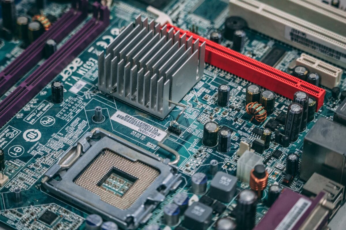
IT decommissioning is the secure process of retiring outdated IT systems, servers, networking equipment, storage devices, and digital infrastructure. The decommissioning process involves:
disconnecting systems,
removing hardware,
destroying sensitive data,
and ensuring assets are recycled, reused, or disposed of according to regulatory requirements.
Businesses carry out IT decommissioning during:
cloud migrations,
office relocations,
infrastructure upgrades,
mergers,
and permanent shutdown projects.
Proper decommissioning activities reduce cybersecurity risks, protect confidential business information, and support safety and environmental standards.
Without a structured decommissioning strategy, organisations may expose sensitive data, fail compliance audits, or create unnecessary environmental risks through improper disposal of hazardous materials.
IT decommissioning helps businesses securely retire old technology, protect sensitive data, reduce operational risks, and comply with environmental and data protection regulations. A professional decommissioning process ensures equipment is safely removed, securely destroyed, and responsibly recycled.
Why IT Decommissioning Is Important
Old IT systems often contain confidential information even after they stop being used. Servers, laptops, storage arrays, backup devices, and networking equipment may still hold:
customer records,
employee information,
financial documents,
and login credentials.
Secure IT decommissioning prevents unauthorised access to this data through administrative and technical controls designed to eliminate security vulnerabilities during equipment removal.
Businesses also benefit from improved operational efficiency. Removing outdated infrastructure frees up physical space, lowers maintenance costs, and supports a more cost-effective IT environment.
For industries such as healthcare, finance, manufacturing, and research, following regulatory controls is essential. Businesses must meet strict regulatory requirements relating to data security, waste disposal, and environmental responsibility.
A detailed risk assessment helps organisations identify operational, environmental, and security threats before decommissioning activities begin.
Understanding the IT Decommissioning Process
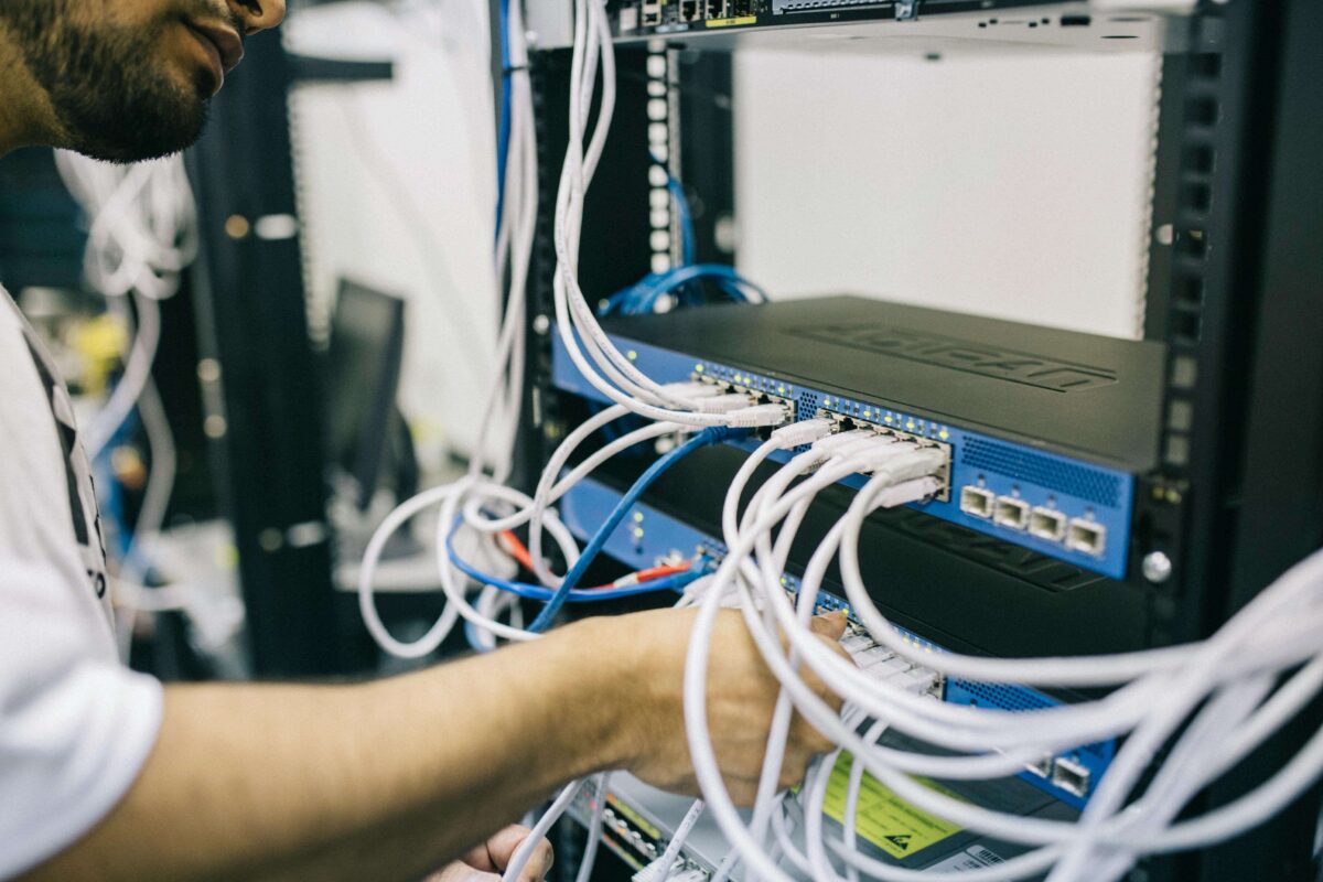
The IT decommissioning process begins with a complete inventory of all equipment scheduled for retirement. Businesses identify servers, desktop computers, storage devices, cables, networking hardware, and other parts of the facility that require removal.
Once assets are identified, critical data is backed up or migrated to replacement systems. This step minimises downtime and ensures business continuity throughout site decommissioning projects.
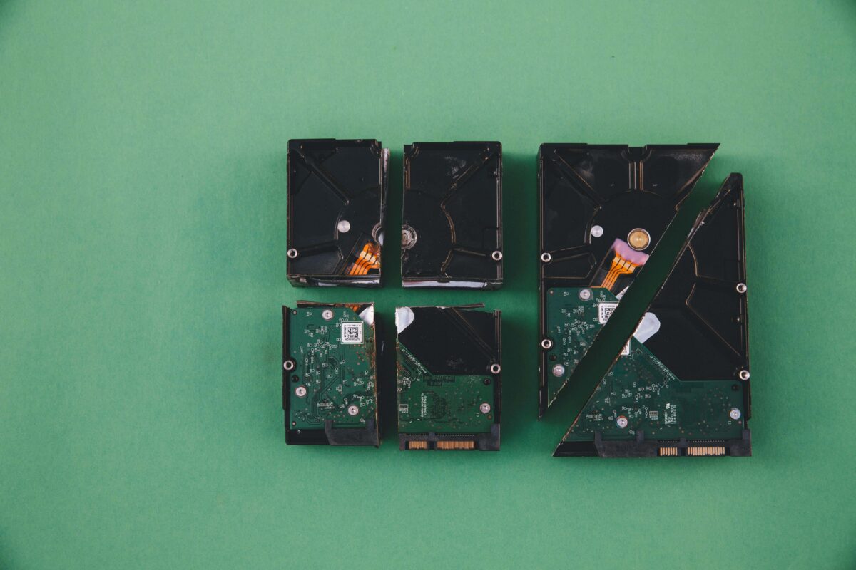
The next stage involves secure data destruction. Certified specialists permanently erase or destroy storage devices using methods such as hard drive shredding, degaussing, and data wiping.
After data destruction, technicians disconnect and remove equipment safely. Devices are inspected to determine whether they can be recycled, reused, or disposed of responsibly through approved waste management channels.
Professional providers then supply audit reports and destruction certificates to confirm that the decommissioning process has been completed according to security and environmental standards.
Secure Data Destruction and Compliance
Data destruction is one of the most important elements of IT decommissioning. Businesses that fail to remove sensitive information correctly may face serious legal, financial, and reputational consequences.
A secure decommissioning strategy includes:
encrypted data handling,
controlled transportation,
and documented destruction procedures.
These administrative and technical safeguards help businesses maintain compliance with GDPR and industry regulations.
Guidance from the Information Commissioner’s Office (ICO) explains how organisations should manage personal and confidential data securely during disposal.
Businesses handling highly sensitive information should also maintain a secure chain of custody during all decommissioning activities.
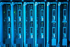
Site Decommissioning and Data Centre Closures
Large-scale site decommissioning projects often involve the removal of entire IT environments. Data centres, office buildings, and industrial facilities may require the coordinated removal of servers, storage systems, cooling infrastructure, and backup power equipment.
A successful decommissioning strategy focuses on operational continuity, security, and environmental compliance. Every stage must be carefully planned to avoid service disruption and minimise risk.
Businesses undergoing permanent shutdown or relocation projects must also evaluate safety and environmental responsibilities before equipment removal begins.
Effective planning ensures all parts of the facility are assessed properly while maintaining compliance with regulatory requirements.
Safety and Environmental Responsibilities
Responsible IT disposal plays a major role in protecting the public and the environment. Many electronic devices contain hazardous materials such as:
lead,
mercury,
lithium batteries,
and chemical components that require specialist handling.
Improper disposal may contaminate landfills, damage ecosystems, and create health risks for local communities.
Businesses involved in scientific research, healthcare, or industrial operations may also manage equipment associated with radioactive material, radioactive substances, or radioactive waste. In these situations, additional regulatory controls and safety procedures are required during long-term decommissioning projects.
Professional decommissioning providers help organisations manage safety and environmental risks while ensuring materials are handled according to legal standards.
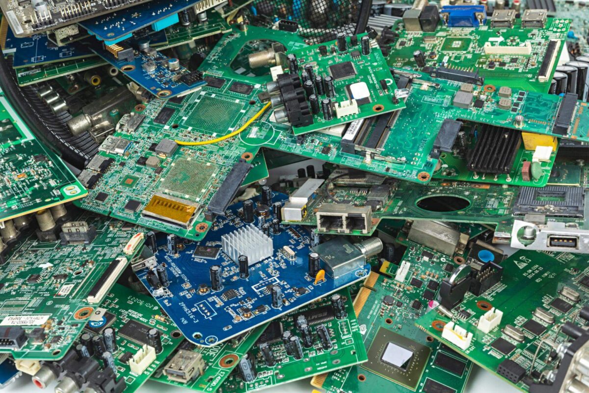
Businesses can also support sustainability goals by ensuring valuable materials are recovered and reused wherever possible.
Benefits of Professional IT Decommissioning
Professional IT decommissioning offers several long-term advantages for organisations of all sizes.
Improved Data Security
Secure destruction methods prevent sensitive information from being recovered or exposed.
Regulatory Compliance
Businesses can meet GDPR, WEEE, and industry-specific regulatory requirements more effectively.
Environmental Protection
Proper disposal methods reduce landfill waste and support environmentally responsible recycling practices.
Reduced Operational Costs
Removing outdated systems creates a more cost-effective IT infrastructure and lowers maintenance expenses.
Better Risk Management
Comprehensive planning and documented procedures reduce operational, environmental, and security risks.
How to Choose the Right IT Decommissioning Provider
Selecting an experienced provider is essential for a secure and compliant project. Businesses should look for companies that offer:
certified data destruction,
detailed reporting,
environmental compliance,
and secure logistics.
Providers should also understand risk assessment procedures, regulatory controls, and long-term infrastructure management requirements.
A reliable decommissioning partner helps businesses complete projects efficiently while protecting sensitive data and supporting environmental sustainability.
What Is IT Decommissioning?
IT decommissioning is the secure process of retiring outdated IT systems and equipment. It includes data destruction, hardware removal, recycling, and compliance management to protect sensitive information and support environmental regulations.
Common queries such as “what is IT decommissioning?” or simply “IT decommissioning?” are addressed here, along with a straightforward overview of the IT decommissioning process.
Conclusion
IT decommissioning is an essential process for businesses retiring outdated technology or upgrading infrastructure. From secure data destruction to responsible recycling, every stage of the decommissioning process supports cybersecurity, compliance, and environmental protection.
By implementing a structured decommissioning strategy, organisations can reduce operational risks, manage hazardous materials safely, and ensure equipment is recycled, reused, or disposed of correctly. Professional decommissioning services also help businesses remain compliant, efficient, and environmentally responsible during long-term infrastructure changes.