How Long Do Printed Circuit Boards Last?
repcb1
on
July 29, 2025
Key Takeaways...
- Average PCB lifespan is 10–20 years, but this varies depending on quality, environment, and usage.
- Exposure to heat, humidity, vibration, and electrical stress can significantly reduce a board’s life.
- Regular maintenance and proper storage can help extend the lifespan of printed circuit boards.
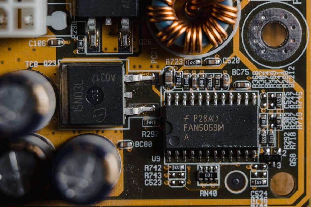
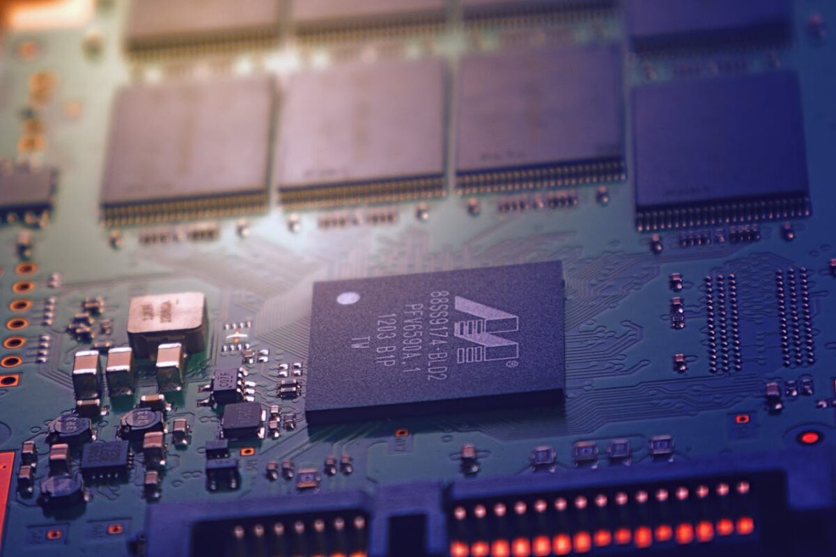
Printed circuit boards (PCBs) are the backbone of modern electronics, providing the essential platform for connecting and supporting electronic components. From consumer devices to industrial equipment, PCBs are built to be robust, but like any technology, they have a finite lifespan.
Understanding how long printed circuit boards last, and the factors that affect their longevity, is crucial for businesses managing electronic assets and planning for end-of-life disposal.
Typical Lifespan of Printed Circuit Boards
On average, a PCB can last anywhere from 10 to 20 years under normal operating conditions. However, this timeframe is influenced by the environment in which the PCB operates, how frequently the device is used, and the quality of the components and materials used in its construction.
In certain high-stress applications, such as heavy industrial machinery or aerospace systems, PCBs may have shorter lifespans due to constant exposure to heat, vibration, and demanding operational cycles.
Conversely, PCBs used in low-stress consumer electronics, which are used intermittently and stored in controlled environments, may last for decades.
Key Factors That Affect PCB Longevity
- Quality of Materials
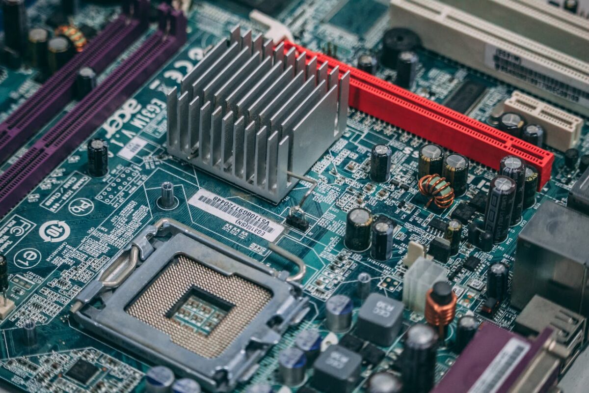
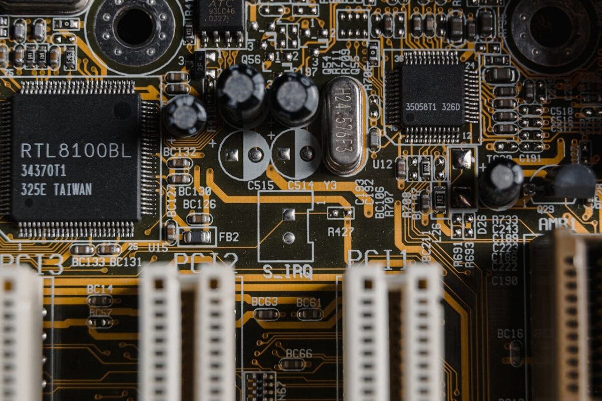
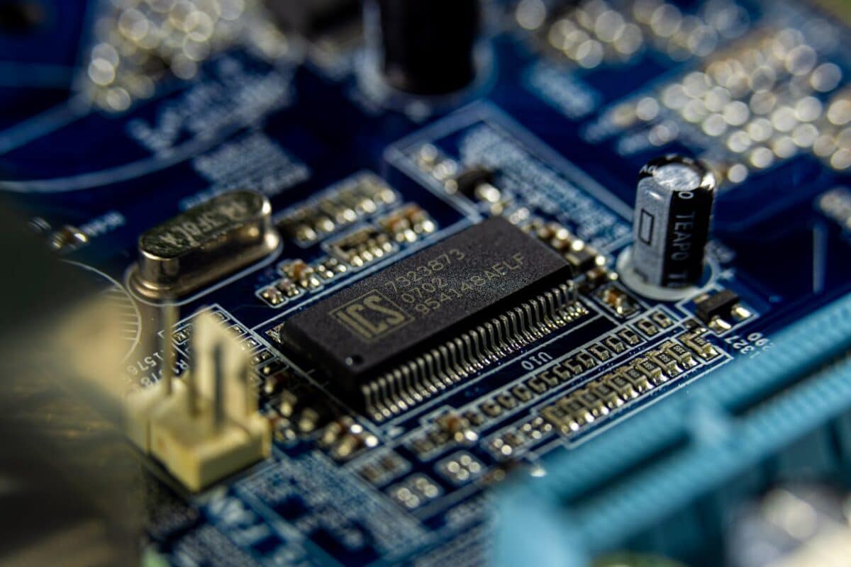
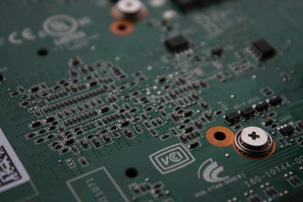
The materials used in the manufacturing of a PCB, including the substrate, copper traces, and solder mask, directly impact durability. High-quality materials resist thermal expansion, corrosion, and physical stress more effectively.
- Operating Environment
PCBs exposed to high humidity, temperature extremes, dust, or corrosive environments will degrade faster. Moisture can lead to corrosion, while excessive heat can cause delamination of the board’s layers or deterioration of solder joints.
- Electrical Stress
Overloading circuits or exposing PCBs to power surges accelerates wear and tear. Electrical stress can cause insulation breakdown and lead to failures in sensitive components.
- Physical Damage
Mechanical stress from vibration, dropping, or improper handling can crack solder joints or damage the PCB substrate. Devices with moving parts or heavy vibration often have reduced board lifespans for this reason.
- Maintenance and Upkeep
Regular cleaning, proper storage, and timely component replacement can prolong a PCB’s life. Dust build-up can cause overheating, while replacing aging capacitors and connectors helps prevent premature failures.
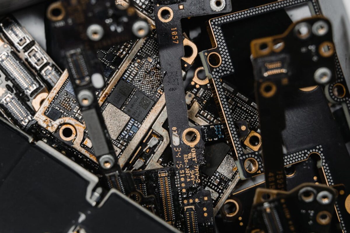
Signs a PCB Is Reaching the End of Its Life
For businesses managing large numbers of electronic devices, it’s helpful to recognise the signs that a PCB is failing or approaching end-of-life. These include:
- Intermittent power issues or device failures
- Visible corrosion or burnt areas on the board
- Bulging or leaking capacitors
- Cracked solder joints or lifted copper traces
- Overheating components
Addressing issues early can prevent costly downtime and data loss, but in many cases, once a PCB is significantly degraded, replacement or recycling becomes the most practical solution.
Responsible End-of-Life Management
When PCBs have reached the end of their usable life, proper disposal is essential. They contain hazardous materials that must be handled in accordance with environmental regulations, as well as valuable metals that can be recovered and reused.
Working with a certified specialist ensures your business stays compliant while supporting the circular economy. At RePCB, we specialise in collecting and recycling PCB waste for businesses across the UK.